Article summary
Recently, we ran into a problem with a new revision of hardware we received for an embedded product. It cost the project 2 days of sleuthing before we found the problem, which ended up being a mixup in the schematic that the PCB was laid out and manufactured according to.
It turned out to be due to an error in the part created in the schematic entry software for a new Zigbee module that we had to migrate to late in the project. It was very disheartening to lose two days tracking down the issue and coming up with a patch. Therefore, I decided to share a few cheap validation methods that we had used at my previous job to keep check on the human element that plagues tedious design/entry work. I hope that sharing these tips will help others not make the same mistakes that caused us to put these measures into place.
Validating New Parts
The Human Factors:
- Part/Package Creation
- Manual Translation to Create Schematic Part from Datasheet
- Pin Locations
- Pin Names/Usages/Polarity
- Tedious/Error-prone
- Manual Translation to Create Schematic Part from Datasheet
- Assigning Signals/Net Names to Pins
- Depends on Package (1) Being Done Properly
- Manual Effort to Convert
- Tedious/Error-prone
The Problem(s):
There are multiple step of schematic and PCB creation that are inherently manual. First, the designer must take pin/signal assignments from a datasheet and create the part for schematic development. Secondly, the physical part/package created for PCB layout is another manual step, and must be coherent with the part in the schematic editor. When there are a large number of new/custom parts in a design, the risk of problems being introduced in these manual steps increase exponentially, in most cases. There has to be a better way to close the loop here!!
Strategies:
In order to acknowledge and deal with the multiple points where manual translation can cause an error, a policy should be put into place where all newly created parts are validated by a separate engineer.
The independent engineer should start directly from the datasheet and validate that each of the following are correct:
- Validate that all of the pins exist in the schematic part, per the datasheet.
- This may lead to pins not being connected at all, and even a rule-checker in the schematic entry software may not catch this.
- Validate that each pin is defined properly, and also that attributes are specified properly to allow the rule checker to perform a more thorough analysis.
- If a pin is assigned incorrectly, this would likely lead to erroneous connections down the line.
- If attributes aren’t set properly on pins, you won’t get the full benefit of design-rule checking. Some examples are:
- A digital pin is specified as analog.
- A power pin is set as analog rather than more explicitly as power, since design-rule check can frequently differentiate between an analog input versus power.
- Pin direction is lazily specified as a bidirectional digital pin, rather than being a dedicated input/output.
- Validate that the physical part package is correct.
- Usually specified as an attribute in schematic entry, which can eliminate a mixup when creating the physical part for PCB layout.
- Use/re-use a standard or known-good package if possible.
- Cross-reference with datasheet.
- Validate with part-pinout diagram for the package type used.
- Double-check that the pinout of the pat in the schematic matches the datasheet.
- Double-check that the pinout is consistent between schematic entry and PCB layout.
- Validate that part rotation is correct and makes sense for interconnects.
- Usually specified as an attribute in schematic entry, which can eliminate a mixup when creating the physical part for PCB layout.
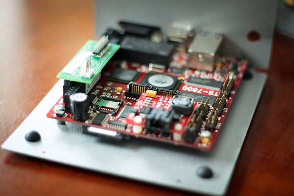
Validating Board-to-Board Interconnects
The Human Factors:
- Engineers Define Pinouts
- Multiple Board Designs Spread across Multiple Engineers
- Depends on (1) Being Done Properly
- Depends on Multiple Engineers Being in Sync
- Cable Routing (via Folds) Can Flip Pinout from One Board to the Other
- Frequently Overlooked
- Depends on (1) and (2) Being Done Properly
Strategies:
Since board-to-board interconnects are frequently non-standard, since we are usually dealing with custom electronics, and since different engineers and/or teams are responsible for interconnecting boards, this is a frequent source of errors. These errors may result in lengthy debugging, necessary manual board hacks, and additional/costly board respins.
Double-checking and low-fidelity paper prototypes can greatly reduce board-to-board interconnect issues. Here is a list of some things to eliminate (or at least help reduce) the occurrence of these errors:
- Have engineers on both ends double-check the connector pinout(s) and/or custom cable schematics to ensure accuracy and consistency.
- Use paper prototypes of cables, and even PCBs, to ensure that cable routing and connection is as desired (especially when cable folds are utilized).
- Annotate the cable paper prototype with key signals:
- Annotate pin #1 and highest pin number (at a minimum) on the paper cable.
- Pay special attention to any signals that switch positions in the interconnect cable from one end to the other.
- Pay special attention to cables which consolidate signals, or have no-connects on a given end of the cable.
- Annotate the cable paper prototype with key signals:
Summary
I hope these tips will help others flush out the interface/interconnect issues prior to spending the money and time to respin boards, especially when in the homestretch of getting a product released. Simulations are a good tool, and hopefully your teams are using simulation to prove out designs as well, though the simple methods noted above are very cheap to implement and well worth the small investment of time.
Are there any other tricks or methods your team uses for electrical design validation and system integration?